Saved Bookmarks
| 1. |
(a) Explain with the help of suitable diagram , the two processes which occur during the formations of a p -n junction diode . Hence , define the terms :(i)depletion region and (ii) potential barrier :(b)Draw a circuit diagram of a p - n junction diode under forward bias and explain its working . |
|
Answer» Solution :(a)(i) Depletion region : Two important processes occur during the formation of - p - n junction :diffusion and drift . Inn type semiconductor , the concentration of electron is more compared to the concentration of holes is more than the concentration of electrons . Duringthe formation ofp - n junction , and due to theconcentration gradient across p - and n - sides holes diffuse from p side to n side and electron diffuse from n - side to p - side . When an electron diffuses from`n to p`, itleaves behind an ionised donor onn side . This ionised doner is immobile as it is bonded to the surrounding atom . When the hole diffuses from` p to n` due to concentration gradiant , it leaves behind an ionised acceptor negative ION .This space charge region on either side of the junction together is known as depletion region. (ii)Barrier potential: When there is a diffusion of holes from p region to n region and diffusion of electrons in the reverse direction takes place , PART ofdepletion layer on n side ofjunction becomes positively charged and the part of depletion layer on p side of the junction becomes negatively charged.Due to this , a junctionpotential is DEVELOPED , which opposes further diffusion of holes and electrons .Hence , this potential acts as a barrier and ISKNOWN as ' barrier potential'. 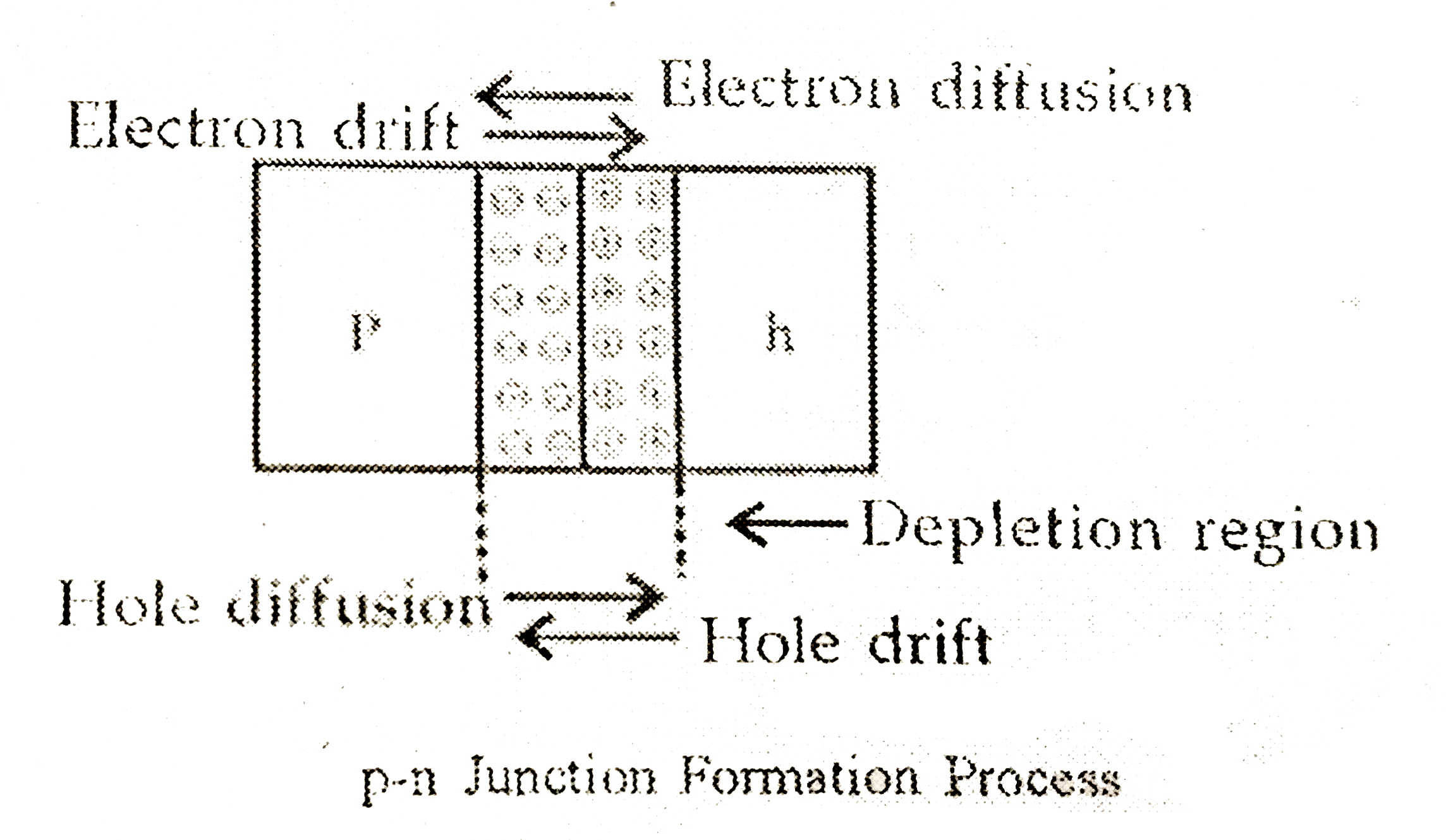
|
|