Saved Bookmarks
| 1. |
Draw the I - V characteristics of Ge and Si pn- junction diodes and explain the same . |
Answer» Solution :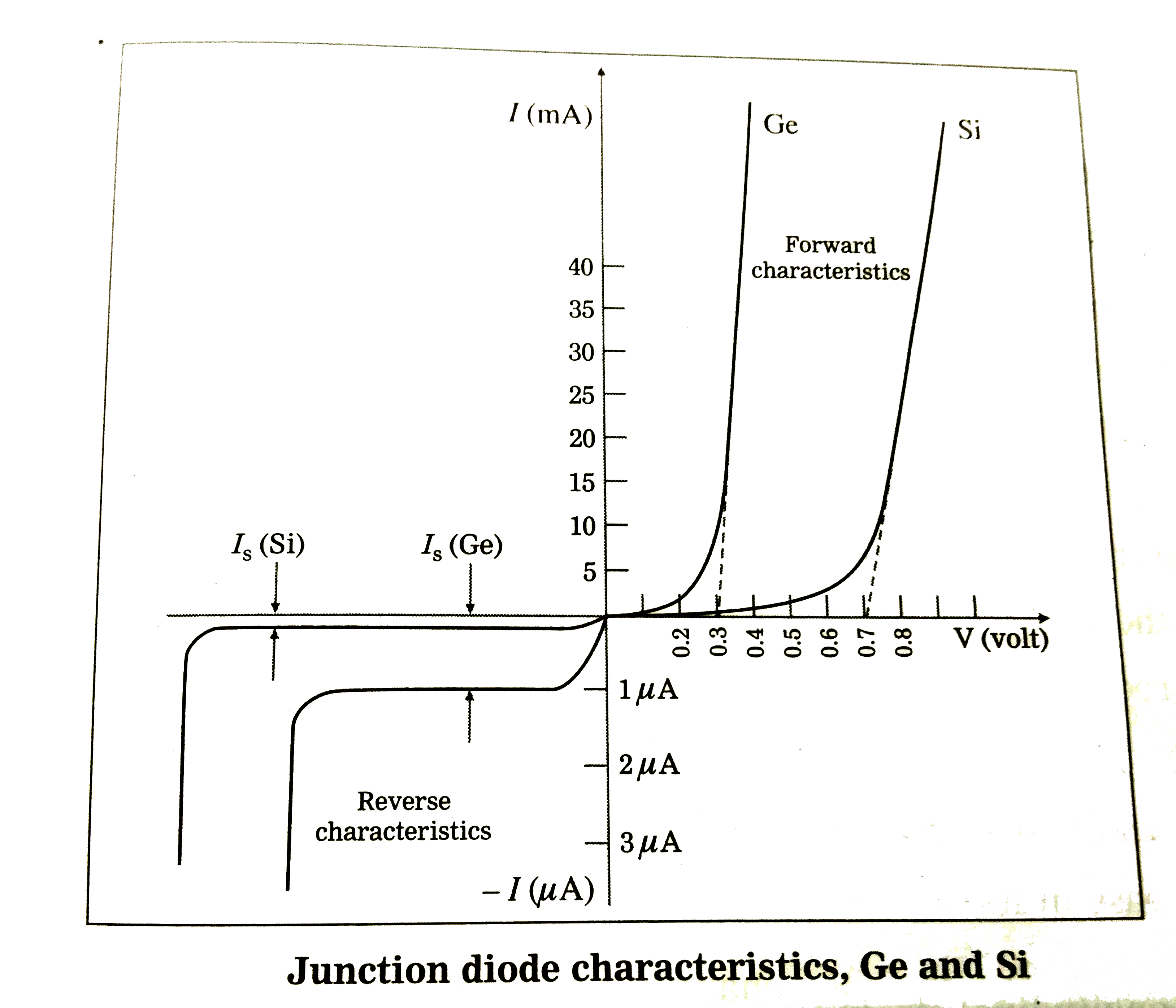 Junction diode CHARACTERISTICS, Ge and Si Explanation : (1) Forward bias characteristics : There is forward current only after the barrier potential of the pn-junction is overcome. Then there is an exponential RISE in the current beyond the knee region. The forward - bias voltage required to reach theregion of upward swing iscalled the threshold voltage `V_(T)` or cut in voltage. When rounded offto the nearest , thethreshold voltage is 0.3 V for a germanium diode and 0.7 V for a silicon diode. (2) Reverse bias characteristics : In the reverse bias, the potential barrier at the junction is large and the current due to majority CARRIERS in each region is zero. However, minority charge carriers are able to cross the junction and CONSTITUTE a very small current in thereverse direction. This reverse current quickly reaches its maximum or saturation value and remains fairlyconstant with increase in thereverse - bias voltage. It is calledthereverse saturation current `I_(s)`, which is typically a few nanoamperes for a silicon diode and a few microamperes for a germanium diode. Too high a negative voltage results in a sharp change in the reverse - bias characteristics. At a CERTAIN characteristic negative voltage, called the peak inverse voltage (PIV) or breakdown voltage, thecurrent in the reverse direction increases very rapidly . In general, a silicon diode has a higher PIV rating `(~1000 V)` than a germanium diode `(~ 400 V)`. |
|