Saved Bookmarks
| 1. |
Draw the labelled circuit diagram of a common-emitter transistoramplifie : Explain clearly how the input and output signals are in opposite phase. |
Answer» Solution :The circuit details for using an npn transistor as common emitter amplifier are shown in the fig. 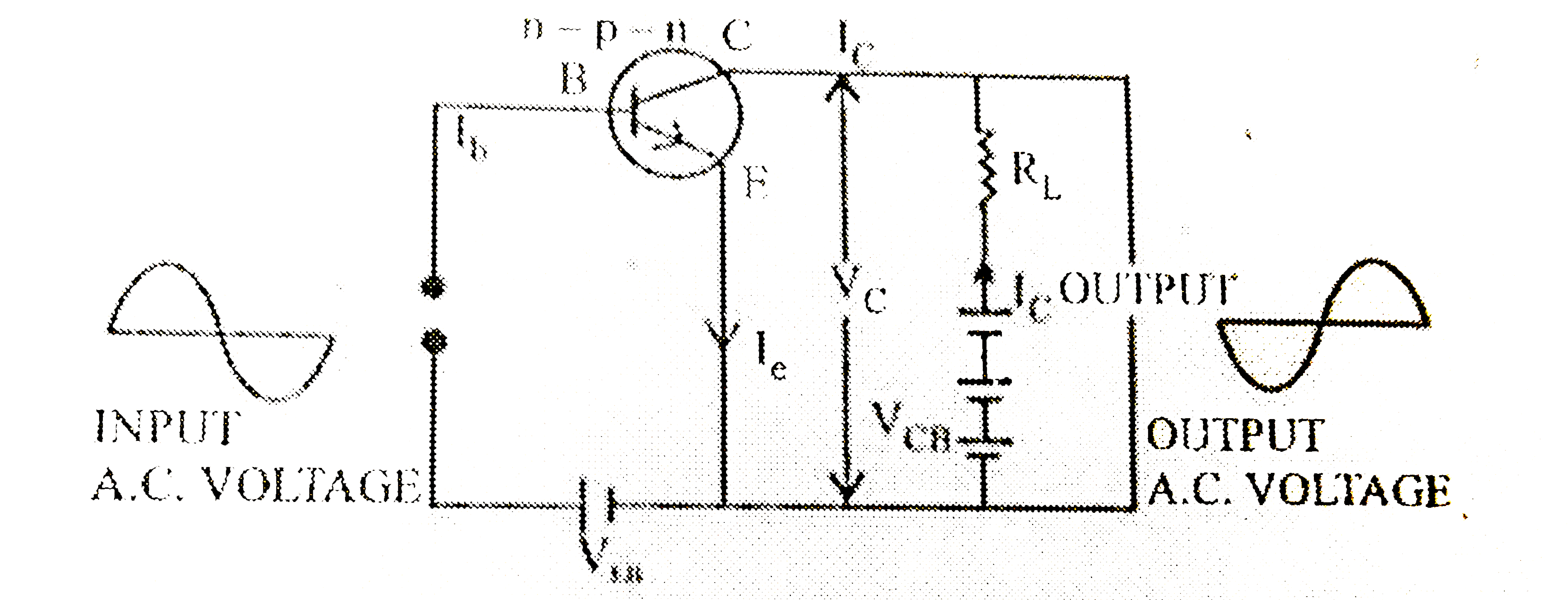 The input (base-emitter) circuit is forward biased and the output (collector-emitter) circuit is reverse biased. When no a.c. signal is applied, the potential difference `V_(c)` between the collector and the emitter , is given by `V_(C)=V_(CE)-I_(C)xxR_(L)` ...(i) Where, `V_(C)` is the voltageof battery `V_(CE)` When an a.c. signal is fed to the input circuit, the forward bias increases during the positive half cycle of the input. This results in an INCREASE in `I_(C)` and a consequent decrease in `V_(C)`, as is clear from (i). THUS during positive half cycle of the input, the collector becomes less positive. During the negative half cycle of theinput, the forward bias is decreased resulting in a decrease in `I_(E)` and hence `I_(C)`. Therefore, from (i) `V_(C)` would increase, MAKING the collector more positive. Hence, in a common-emitter amplifier, the output voltage is `180^(@)` out of phase with the input voltage. |
|