Saved Bookmarks
| 1. |
(i) Draw a circuit diagram to study the input and output characteristics of an n-p transistor in its common emitter configuration. Draw the typical input and output characteristics. (ii) Explain, with the hepl of a circuit diagram, the working of n-p transistor as a common emitter amplifier. |
|
Answer» Solution :(i) The circuit arrangement to obtain the characteristics of a n-p transistor is shown in figure. Input characteristic : Input characteristics are graph between `V_(BE) and I_(B)` at constant `V_(CE)` Output characteristics : Output characteristics are graph between `V_(CE) and I_(C)` at constant `I_(B)` 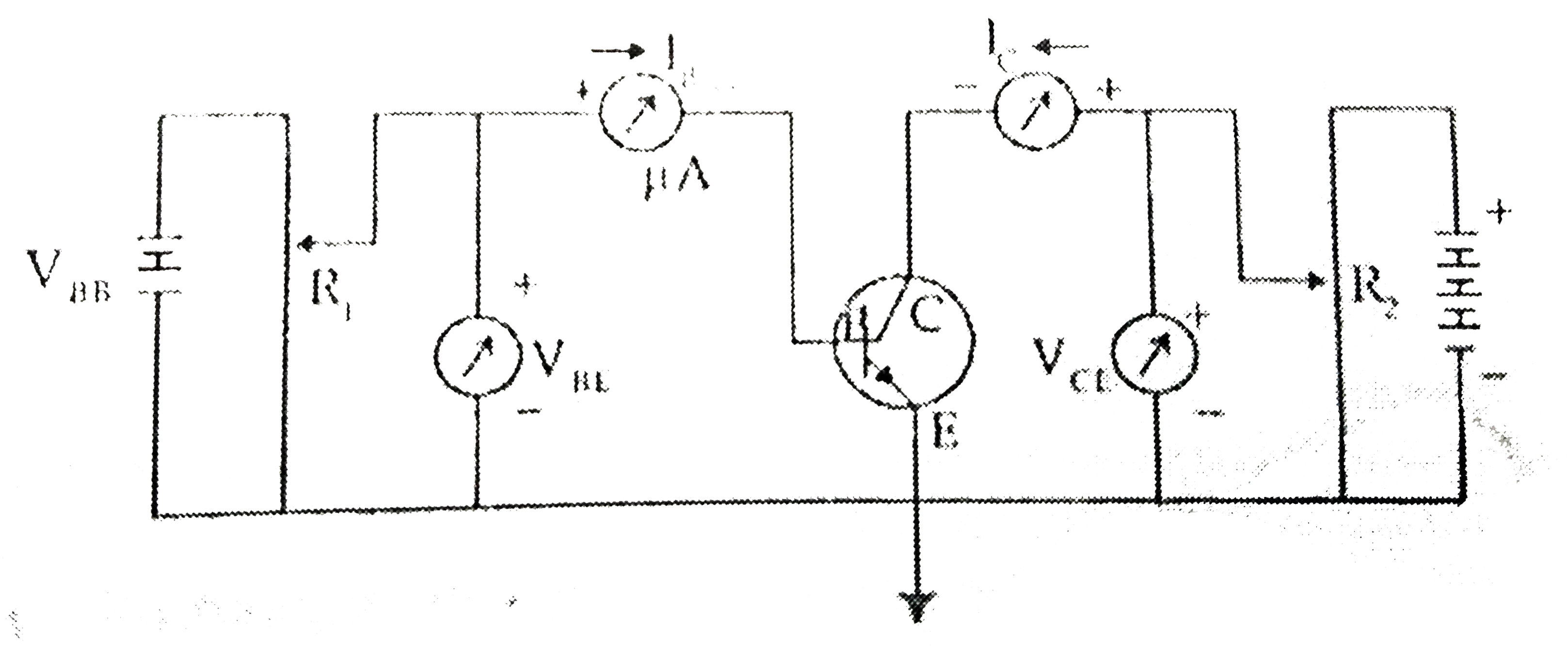 (ii) Transistor amplifier is based on the principle that a WEAK input signal given to base region produces an amplified (LARGE) output signal in the collector region. 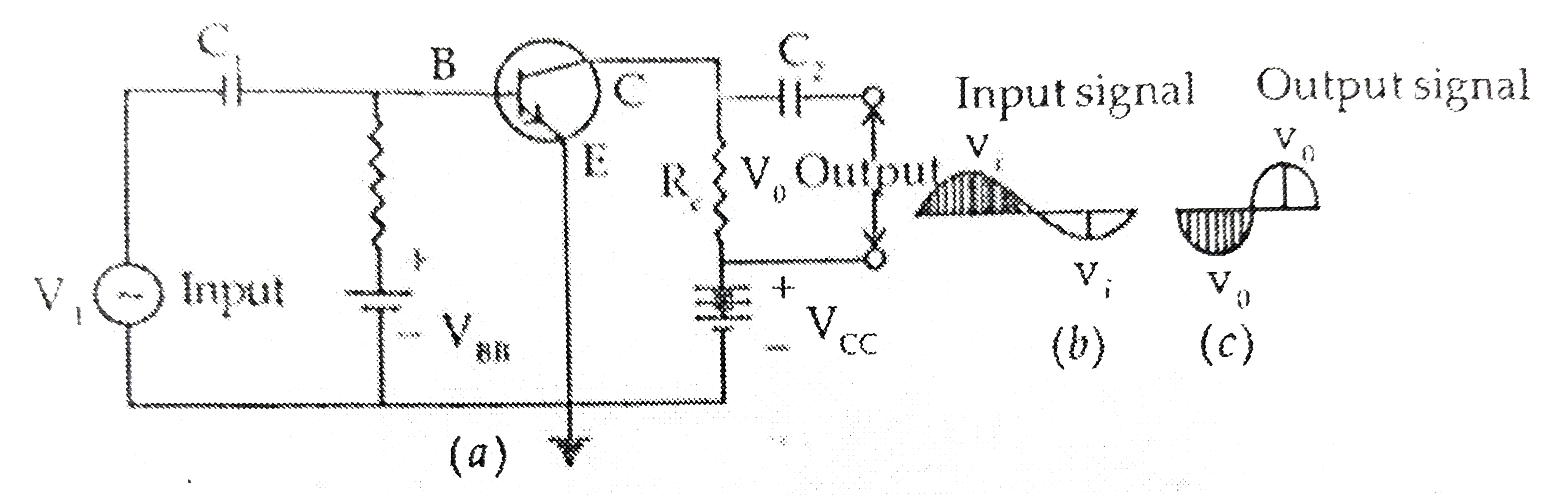 A simple amplifier circuit in common emitted configuration using a n-p-n transistor has been shown in Fig. The input signal `v_(i)` is CONNECTED between base and emitter through a capacitor `C_(1)`, which blocks d.c. voltage VBB from going towards the a.c. input source. The output is taken from the collector resistance RC. The capacitor `C_(2)` blocks the d.c. voltage VCC from the output signal `v_(0)` Due to input signal the base current changes by a value `i_(B) = (v_(i))/(R_(B))` and correspondingly collector current changes by `i_(C) = beta i_(B) = beta (v_(i))/(R_(B))` `:.` Output voltage ACROSS RC will be `v_(0) = R_(C).i_(C) = beta (R_(C))/(R_(B)) v_(i) or " Voltage gain " A_(v) = (v_(0))/(v_(i)) = beta.(R_(C))/(R_(B))` The input and output wavefronts have been shown in fig.(b) and (c), respectively. The output is amplified but is in opposite phase i.e., the input differ in phase by `180^(@) or pi` radian. |
|